📢 $9.99 flat rate shipping in EMEA countries! Ends May 15th - Don't Miss Out!. 🛒 Shop now
Active
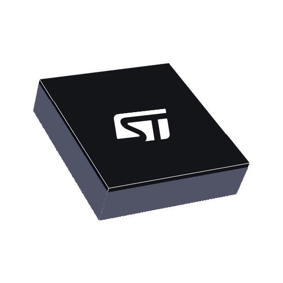
EMIF08-VID1F3
8-line low capacitance EMI filter and ESD protection
| Operating Temp Min Celsius | 85.0 |
| Operating Temp Max Celsius | -40.0 |
| ECCN US | EAR99 |
| ECCN EU | NEC |
| Package Size | 3.14 x 1.035 x 0.60 |
| Packing Type | Tape And Reel |
| RoHs compliant | Ecopack2 |
| Grade | Industrial |
| Package Name | CSP P 0.4 mm |
This is a highly integrated 8-line device designed to suppress EMI/RFI noise in all systems exposed to electromagnetic interference.
This filter includes ESD protection circuitry, which prevents the application from damages when subjected to ESD surges up to 20 kV.
|
Out of Stock
| Quantity | $ per unit | Savings |
|---|---|---|
| 1-9 | $0.57 | 0% |
| 10-24 | $0.55 | 4% |
| 25-49 | $0.53 | 7% |
| 50-99 | $0.43 | 24% |
| 100-249 | $0.39 | 32% |
| 250-499 | $0.36 | 38% |
| 500 | $0.34 | 41% |
| 500 + |
Contact sales |
|
$0.57
| Operating Temp Min Celsius | 85.0 |
| Operating Temp Max Celsius | -40.0 |
| ECCN US | EAR99 |
| ECCN EU | NEC |
| Package Size | 3.14 x 1.035 x 0.60 |
| Packing Type | Tape And Reel |
| RoHs compliant | Ecopack2 |
| Grade | Industrial |
| Package Name | CSP P 0.4 mm |
This is a highly integrated 8-line device designed to suppress EMI/RFI noise in all systems exposed to electromagnetic interference.
This filter includes ESD protection circuitry, which prevents the application from damages when subjected to ESD surges up to 20 kV.
|

