🎉 Exclusive offer: FREE shipping of all MCU & MPU products. No code or minimum required. 🛒 Order now!
📢 Bonus offer: Get our latest VIPGAN65 board with Free shipping. Use code DV-EVLVIPGAN65DF-FREESHIP-05 at checkout! 🛒 Claim now!
Active
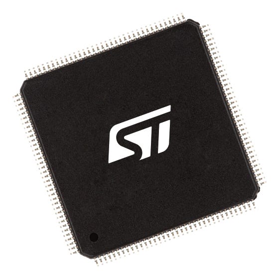
STM32H7B0ZBT6
High-performance and DSP with DP-FPU, Arm Cortex-M7 MCU with 128KBytes of Flash memory, 1376 KB SRAM, 280 MHz CPU, L1 cache, graphic accelerations, external memory interfaces and large set of peripherals
| Supply Voltage Min Volt | 1.62 |
| Supply Voltage Max Volt | 3.6 |
| Operating Temp Min Celsius | -40.0 |
| Operating Temp Max Celsius | 85.0 |
| Core | Arm Cortex-M7 |
| ECCN US | 5A992.c |
| ECCN EU | NEC |
| Packing Type | Tray |
| RoHs compliant | Ecopack2 |
| Grade | Industrial |
| Package Name | LQFP 144 20x20x1.4 mm |
STM32H7B0xB devices are based on the high-performance Arm® Cortex®-M7 32-bit RISC core operating at up to 280 MHz. The Cortex® -M7 core features a floating point unit (FPU) which supports Arm® double-precision (IEEE 754 compliant) and single-precision data-processing instructions and data...
Read More
|
| Quantity | $ per unit | Savings |
|---|---|---|
| 1-9 | $14.14 | 0% |
| 10-24 | $10.75 | 24% |
| 25-49 | $10.32 | 27% |
| 50-99 | $10.30 | 27% |
| 100-249 | $9.08 | 36% |
| 250-359 | $7.78 | 45% |
| 360-10000 | $7.38 | 48% |
| 10000 + |
Contact sales |
|
| Supply Voltage Min Volt | 1.62 |
| Supply Voltage Max Volt | 3.6 |
| Operating Temp Min Celsius | -40.0 |
| Operating Temp Max Celsius | 85.0 |
| Core | Arm Cortex-M7 |
| ECCN US | 5A992.c |
| ECCN EU | NEC |
| Packing Type | Tray |
| RoHs compliant | Ecopack2 |
| Grade | Industrial |
| Package Name | LQFP 144 20x20x1.4 mm |
STM32H7B0xB devices are based on the high-performance Arm® Cortex®-M7 32-bit RISC core operating at up to 280 MHz. The Cortex® -M7 core features a floating point unit (FPU) which supports Arm® double-precision (IEEE 754 compliant) and single-precision data-processing instructions and data...
Read More
|


