STM32H753VIH6

STM32H753VIH6

Active

Free

STM32H753VIT6

High-performance and DSP with DP-FPU, Arm Cortex-M7 MCU with 2MBytes of Flash memory, 1MB RAM, 480 MHz CPU, L1 cache, external memory interface, JPEG codec, HW crypto, large set of peripherals

Supply Voltage Min Volt1.71
Supply Voltage Max Volt3.6
Operating Temp Min Celsius-40.0
Operating Temp Max Celsius85.0
CoreArm Cortex-M7
ECCN US5A992.c
ECCN EUNEC
Packing TypeTray
RoHs compliantEcopack2
GradeIndustrial
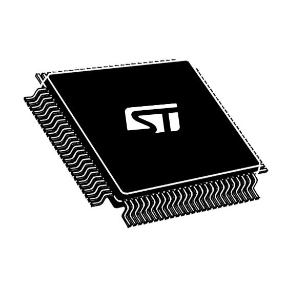
Package NameLQFP 100 14x14x1.4 mm

STM32H753xI devices are based on the high-performance Arm® Cortex®-M7 32-bit RISC core operating at up to 480 MHz. The Cortex® -M7 core features a floating point unit (FPU) which supports Arm® double-precision (IEEE 754 compliant) and single-precision data-processing instructions and data...
Read More

Key features
  • Core
    • 32-bit Arm® Cortex®-M7 core with double-precision FPU and L1 cache: 16 Kbytes of data and 16 Kbytes of instruction cache; frequency up to 480 MHz, MPU, 1027 DMIPS/ 2.14 DMIPS/MHz (Dhrystone 2.1), and DSP instructions
  • Memories
    • 2 Mbytes of Flash memory with read-while-write support
    • 1 Mbyte of RAM: 192 Kbytes of TCM RAM (inc. 64 Kbytes of ITCM RAM + 128 Kbytes of DTCM RAM for time critical routines), 864 Kbytes of user SRAM, and 4 Kbytes of SRAM in Backup domain
    • Dual mode Quad-SPI memory interface running up to 133 MHz
    • Flexible external memory controller with up to 32-bit data bus: SRAM, PSRAM, SDRAM/LPSDR SDRAM, NOR/NAND Flash memory clocked up to 100 MHz in Synchronous mode
    • CRC calculation unit
  • Security
    • ROP, PC-ROP, active tamper, secure firmware upgrade support, Secure access mode
  • General-purpose input/outputs
    • Up to 168 I/O ports with interrupt capability
  • Reset and power management
    • 3 separate power domains which can be independently clock-gated or switched off:
      • D1: high-performance capabilities
      • D2: communication peripherals and timers
      • D3: reset/clock control/power management
    • 1.62 to 3.6 V application supply and I/Os
    • POR, PDR, PVD and BOR
    • Dedicated USB power embedding a 3.3 V internal regulator to supply the internal PHYs
    • Embedded regulator (LDO) with configurable scalable output to supply the digital circuitry
    • Voltage scaling in Run and Stop mode (6 configurable ranges)
    • Backup regulator (~0.9 V)
    • Voltage reference for analog peripheral/VREF+
    • Low-power modes: Sleep, Stop, Standby and VBAT supporting battery charging
  • Low-power consumption
    • VBAT battery operating mode with charging capability
    • CPU and domain power state monitoring pins
    • 2.95 μA in Standby mode (Backup SRAM OFF, RTC/LSE ON
In stock
Quantity $ per unit Savings
1-9$15.920%
10-24$14.598%
25-99$11.8626%
100-249$11.6627%
250-539$10.6733%
540-10000$9.9538%
Contact sales
$15.92
$15.92
or
Supply Voltage Min Volt1.71
Supply Voltage Max Volt3.6
Operating Temp Min Celsius-40.0
Operating Temp Max Celsius85.0
CoreArm Cortex-M7
ECCN US5A992.c
ECCN EUNEC
Packing TypeTray
RoHs compliantEcopack2
GradeIndustrial
Package NameLQFP 100 14x14x1.4 mm

STM32H753xI devices are based on the high-performance Arm® Cortex®-M7 32-bit RISC core operating at up to 480 MHz. The Cortex® -M7 core features a floating point unit (FPU) which supports Arm® double-precision (IEEE 754 compliant) and single-precision data-processing instructions and data...
Read More

Key features
  • Core
    • 32-bit Arm® Cortex®-M7 core with double-precision FPU and L1 cache: 16 Kbytes of data and 16 Kbytes of instruction cache; frequency up to 480 MHz, MPU, 1027 DMIPS/ 2.14 DMIPS/MHz (Dhrystone 2.1), and DSP instructions
  • Memories
    • 2 Mbytes of Flash memory with read-while-write support
    • 1 Mbyte of RAM: 192 Kbytes of TCM RAM (inc. 64 Kbytes of ITCM RAM + 128 Kbytes of DTCM RAM for time critical routines), 864 Kbytes of user SRAM, and 4 Kbytes of SRAM in Backup domain
    • Dual mode Quad-SPI memory interface running up to 133 MHz
    • Flexible external memory controller with up to 32-bit data bus: SRAM, PSRAM, SDRAM/LPSDR SDRAM, NOR/NAND Flash memory clocked up to 100 MHz in Synchronous mode
    • CRC calculation unit
  • Security
    • ROP, PC-ROP, active tamper, secure firmware upgrade support, Secure access mode
  • General-purpose input/outputs
    • Up to 168 I/O ports with interrupt capability
  • Reset and power management
    • 3 separate power domains which can be independently clock-gated or switched off:
      • D1: high-performance capabilities
      • D2: communication peripherals and timers
      • D3: reset/clock control/power management
    • 1.62 to 3.6 V application supply and I/Os
    • POR, PDR, PVD and BOR
    • Dedicated USB power embedding a 3.3 V internal regulator to supply the internal PHYs
    • Embedded regulator (LDO) with configurable scalable output to supply the digital circuitry
    • Voltage scaling in Run and Stop mode (6 configurable ranges)
    • Backup regulator (~0.9 V)
    • Voltage reference for analog peripheral/VREF+
    • Low-power modes: Sleep, Stop, Standby and VBAT supporting battery charging
  • Low-power consumption
    • VBAT battery operating mode with charging capability
    • CPU and domain power state monitoring pins
    • 2.95 μA in Standby mode (Backup SRAM OFF, RTC/LSE ON